In addition to structural dimensions of individual selected structures also the determination of existing defects on the wafer is necessary for process control in semiconductor industry. From knowledge of the defect density, defect types and their distribution, action can be taken to increase yield of a specific process. For such measurement tasks the method of scatterometry is inappropriate because it’s too slow for measuring representative sets of structures on an entire wafer.
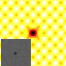
With the help of defectoscopy, however, one can quickly investigate a large number of structures simultaneously. For this purpose a microscopic setup is used, which cannot provide a fully resolved image of these structures anymore. An advantageous feature of defects compared to structures is, that in practice defects occur in isolation, which means that in a periodic array of identical structures significantly different optical properties are present in isolated areas. Under certain lighting conditions, these objects appear as bright or dark pixels in the microscopic image, regardless of how large the structures or defects are. These lighting conditions can then be used as a specific signature to distinguish between different defects. These signatures can be developed together with the introduction of a new process using rigorous simulations.
Publications
- S. Rafler; T. Schuster; K. Frenner; W. Osten; U. Seifert: Improvements on the simulation of microscopic images for the defect detection of nanostructures, Proc. SPIE 6922 (2008) 692215
- S. Rafler; M. Petschow; U. Seifert; K. Frenner; W. Osten: Effects of Pupil Discretization and Littrow illumination in the Simulation of Bright-field defect detection, Optics Letters 34, Issue 12, p. 1840 (2009)