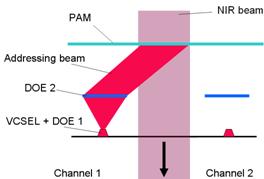
The scope of this project is the development of a compact micro optical device (Fig. 1) for non-pixelated spatial polarisation control.

Fig. 1: Schematic diagram of the basic setup
The device in Fig. 1 is based on a photoaddressable material (PAM) witch transfers the shape of the optical addressing beam into a spatially shaped polarization pattern. The change in polarization depends on the polarization and intensity of the addressing light. The addressing is done with red light (655 nm), the usable wavelengths for polarization manipulation lie in the near infrared (NIR).
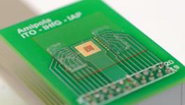
The micro optical addressing module (Fig. 2) uses VCSELs as light sources and two diffractive optical elements (DOE) for beam shaping. Due to the small dimensions of the illumination system, several addressing channels can be realised in one device. By controlling the current through the VCSELs, different illumination patterns can be switched or combined.

Fig. 2: Diffractive optical addressing module with 4 different switchable addressing patterns
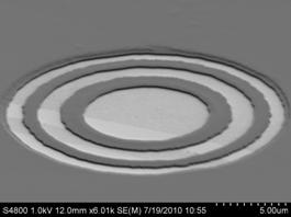
The first DOE is directly integrated on the VCSEL surface and is used for course beam shaping to optimize the illumination for the second, larger DOE. The DOEs on the VCSEL surface can be realized as phase or amplitude elements, the sample shown in Fig. 3 is an amplitude element.

Fig. 3: Fresnel zone plate directly etched into the VCSEL surface (IHFG, Uni Stuttgart)
Further work will focus on the generation and test of more complex DOEs on the VCSEL surface, the use of optimized PAM (higher induced birefrin-gence and faster response), the extension to larger addressing areas and the application in phase contrast microscopy.
Supported by: DFG OS111/26-1
This project is part of the DFG priority pro-gramme 1337 “active micro optics” and is done in collaboration with the IHFG (University Stuttgart) and University Potsdam.

